I wanted to build an Internet of Things (IoT) device while also improving my skills in microcontrollers and in design. The main goal was to make a simple device while also being both a useful exercise and robust/usable product. With this in mind, I designed and built widget which connects to the internet, polls a website for a JSON, extracts a specific number (for example the experimental shot number or air quality index) and displays it via an SPI-connected 8-digit 7-segment display. The finished product feels like the 21st century equivalent of a bed-side clock, but with much more versatility. This project really highlights the revolution in design allowing for a hobbyist to make complicated products while maintaining both a low development cost and a fast design process.
Doing this required three different segments: designing an integration between the two main electronic components, a housing to mate these components, and code to drive the whole device.
This required solutions for the following challenges:
- Proper design tolerancing of parts for print variability and poor electronics workmanship
- PCB design which matches physical and electrical requirements at 3.3 and 5V
- Using the C-based workflow to properly utilize the ESP-01
As it might seem that each problem is distinct and that these challenges are given chronologically, that was not the case. Each are significantly interrelated, where physical constraints impacted the electronic design which in turn changed the way in which the microcontroller would be programmed. The PCB design and case CAD design did progress before the actual coding, but after the general characteristics of the microcontroller control were defined. Overall, this project was enjoyable in the necessary problem solving, but also allowed me to take pride in the quality and finish of the end product.
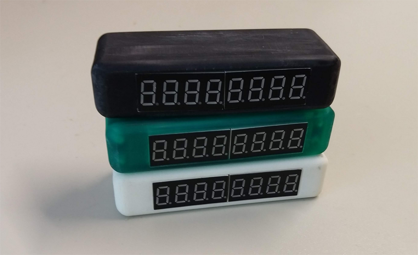
3D printing of a compact housing
One of the great selling points of any 3D printer is the overall accuracy in creating extremely complex components. However, as with all design and manufacturing, the devil is in the details. The precision defines the overall print tolerance, or the printer’s ability to minimize errors in component (especially errors as it relates to others). Extra care had to be taken to predict errors/tolerance problems that were likely to exist, namely in mating the components and in integration the various printed circuit boards. Finally, I also wanted the end result to be rigid, rugged, and stylish. This meant that the end result needed clean lines, smooth curves and close fitting components.
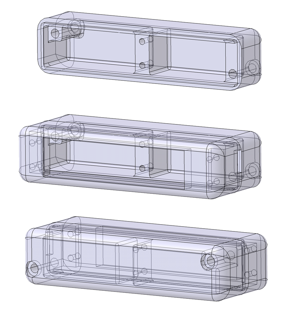
All of the PCBs (the 7 segment display, the ESP8266 microcontroller and the mating board which contains power and communication) must be robustly fastened within the case, with the display cleanly matching the case design. The .56” 7-segment display and ESP8266 are both cheap and easy to acquire components, approximately $3 each on Amazon respectively. However, the cost and availability come at the cost in their tolerances, making it a difficult problem. This is readily observable in the exterior design which had to take the tolerance issues into account while staying aesthetically pleasing. Fitting both of these requirements took significant time (hands off to product designers, that stuff is not easy).
The display PCB’s 8 digits are separated into two 4 segment pieces. These pieces are roughly soldered in, and are often misaligned from one another by an angle or offset. As seen in the CAD drawings, only 2 of the four screw holes of the display were used to screw the housing together. The other two were for attaching the display to the front housing. Interestingly. these threaded holes are not centered within the housing due to the display PCB design, as the display is offset to one side of the display PCB.
The tolerance problems of the display highlight the difficult nature of a multiple part design. The rectangular hole for the display has an additional millimeter gap to account for poor PCB construction. Error in the digit placement impacts at minimum 3 other dimensions on the front housing. This also shows that even for simple projects such as this, that the complex nature of manufacturing leads to significantly more difficulty in the design.
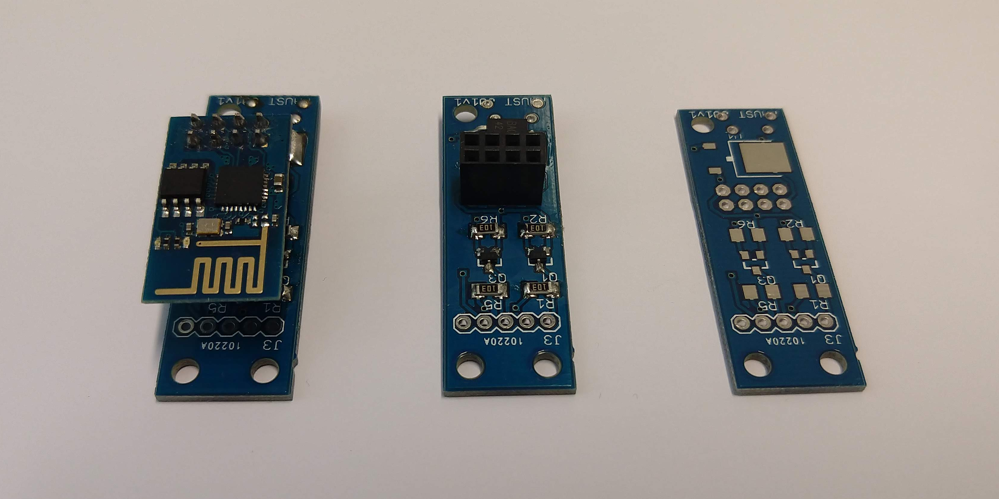
The other two PCBs (the ESP8266 and interface boards) are screwed into back half. The two segments (the display and interface) are electrically connected by 5 1” wires. This allows flexibility in the final assembly. Similar to the display, only two screws attach the interface board to the housing, but the interface board has a header to connect the ESP8266. The surface of the interface board is set so that the Micro USB connector can sit nearly flush with the side of the housing. Together the two 3D printed pieces make the necessary hole for the USB connector. However, the dimensioning of this hole was made larger than necessary since I didn’t trust my ability to surface mount solder accurately.
The ESP8266 board has a slightly smaller width than the interface board so that it can be recessed farther back in the housing. While this made sense from a mechanical design prospective, updating the flash on the microcontroller requires removing four of the six screws. This makes changing the WiFi network a pain and is definitely something I would do differently if I were to redesign it. The design also has a significantly large, useless void on the opposite side of the two boards which could be replaced by a battery in a future iteration.
The very thick nature of the device is really a product of the interfaces between the PCBs. The display required it to be wired, and the ESP8266 required the use of a header. Headers are inherently very large and contributed greatly to the overall size. I now understand why there is such focus on single board phones and computers, and specialty connectors for components, as these greatly impact the thickness of the device. In this case the overall size and weight make it much more suitable for a desk, rather than something in a pocket.
The housing pieces were first printed in sintered nylon and later versions in resin. I am experienced with PLA printers from other 3D printing projects, but I wanted to learn more about the accuracy, precision, and requirements of these other printing styles. The nylon tends to accrue dirt easily due to the surface finish (as can be seen in some photos) and is a bit expensive. The resin is very high quality in precision (even though my printing service significantly scuffed the exterior) and the surface is still very smooth (better than PLA and nylon). However, it is much more rigid. Tapping the holes is necessary in resin rather than forcing in the M3 screws, which I often do in PLA and nylon. The error in these prints were less than .25mm, meaning that mating surfaces should be toleranced with .5mm. This allowed for solid mating while also preventing too much ‘play’. Both nylon and resin allow for very small features which is knowledge I will certainly use in the future.
Designing and building an interfacing circuit board
The interfacing board was truly the hardest part of the entire process. It is what links the programming to the physical design, bringing all of the various design pieces together. It contains constraints from the mechanical design (such as the additional through hole), to the programming (3 outputs), to the electronic (the necessary 5V 3.3V level shifting). It was also my first personal attempt at ordering and negotiating with a PCB print house, which was previously done by my technicians in my labs. It was very much a learning experience where the order of development is important for reducing cost.
When developing the schematic, it should be done concurrently with the shopping for circuit elements. For example, the micro USB connector was very expensive as the available pad in EAGLE was meant only for Molex connectors. Other, different layouts would have saved money and simplified ordering. As an aside and unbeknownst to me at the time, ordering specialty circuit components, especially surface mount components, are very difficult in Germany due to tax laws. Many of the typically large electronic sellers will simply not sell to individuals as it is prohibitively expensive and complicated. As a hobbyist, this really drives up cost and stifles innovation. I expect that hackerspaces or community labs have some sort of corporate tax number to avoid this problem.
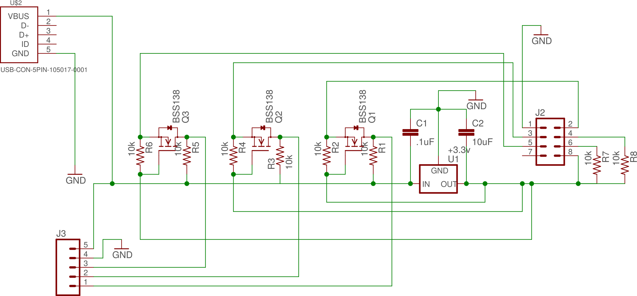
The greatest concern early on was figuring the power and voltage requirements of the circuit. The ESP8266 uses 3.3V logic and will become damaged with 5V input. On the other hand, the display uses 5V. I decided due to simplicity to base the whole device around micro USB due to the availability of chargers, but is a 5V standard. This necessitated the use of a regulator and three level shifters. I simply based the level shifting circuit of a Adafruit breakout board, which is straightforward and uses cheap components.
The 7 segment display uses an SPI interface without a MISO line. This means 3 output pins talk from the ESP8266 to the MAX7221, and the remaining two providing power and ground. The power can be directly linked from the USB to the display, and almost all other circuit components are used to isolate/translate the 3.3V functionality of the ESP8266.
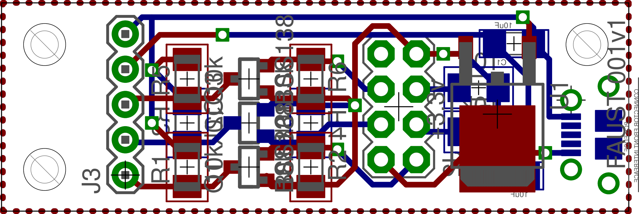
Soldering surface mount components with a typical soldering iron takes practice and dexterity. Assembling each board does take significant time, although it was good practice. There are great guides online to doing it this way, and is a useful repair skill to know. The key is to only solder one pad, attach the surface component in the right position with that pad, and then solder the other pad to finish. This makes it flat and in the right orientation with a strong connection. I purposefully chose larger elements to simplify my soldering (1206), which made for a larger board than necessary. However, these sacrifices did serve to simplify assembly.
Designing circuit boards cheaply require that they be 1) small 2) two layers and 3) of standard thickness. It also helps that free PCB CAD softwares often have size limitations. Due to the small nature of this project by size, this worked quite well to keep the price down. A lot of cheap houses are in China and have month long turn around times which was perfectly acceptable in this case. I used Seeed Studio due to its cheap costs, clear instructions, and professional nature.
Since I could only roughly estimate the necessary current needed to operate the device, and with an aversion to capactive coupling, I designed the traces to be wide and widely separated. The slow communication speed I utilizes (~1 kHz) was more than enough for this application. The overall current draw was lower than I expected (nothing gets hot), so it is way overbuilt. Future iterations would not need as powerful a regulator, and the board itself could probably be reduced in s ize.
Writing the microcontroller C code
When I first conceptualized the necessary components for this project, the implementation of Arduino-based ESP8266 control was still in its infancy. Initially, I wanted the WiFi to connect to the rather ubiquitous Eduroam network, of which a github user joostd provided the necessary interface. I discovered later that the ESP8266 only functions for the WPA2 PSK version with MSCHAPv2 verification protocol, which my workplace’s EDUROAM (and other locations) does not use. In any case, as a way of forcing myself to learn in depth about microcontrollers I chose to avoid the simplicity provided by Arduino.
An open-source framework built around the Espressif SDK was available by another GitHub user named pfalcon. This repository gives all the necessary components and the guide necessary to compile and flash to the ESP8266 microcontroller. The code is, like for most other microcontrollers, in C. My previous experience with C made the step to microcontrollers less abrupt. Additionally the compiler is gcc-like, with the flashing utility written in Python, both solidly in my comfort-zone. This functionality (luckily) was meant for use on Linux machines, making it a useful step towards proper microcontroller development.
While the pin control is easily accessible in the SDK, physically the native SPI interface pins are not available on the ESP-01 (as described earlier). I had to write a bit-banging interface to the MAX7221 7-segment control chip. This code is stored separately from the other code for overall readability. This was really key for debugging the later http requests, as simple response codes could tell me the degree of success.
The key to programming the ESP8266 with the open-SDK is that all work should be moved to the flash if entirely possible. Save for some special circumstances (which is excellently described in this blog post), all functions should have “icache_flash_attr” in front to save RAM. While I didn’t explicitly need it, there are ways of also doing similar movements of variables as well.
That being said, some of the pre-compiled SDK libraries do not use follow this convention and therefore eat a lot of the available RAM. Even without much of my code, by just including the necessary libraries for the esphttpsclient (such as ssl), JSON and WiFi libraries together was enough to exceed the RAM limit. As a solution I chose to rebuild the JSON package with the “icache_flash_attr” flag to get the RAM requirement under the limit. I was able to deduce that Espressif had utilized the Contiki-os JSON parser from their header files, again making my job relatively easy. While my code is not complex, the RAM requirements needed for a larger project highlights the need for clever coding.
Finally, I must say that this project really does hinge on the work of GitHub user Caerbannog, who did all of the legwork of writing an HTTP GET and HTTP POST code for the Espressif SDK. While initially I thought this portion of the code would take significant time to debug and validate, it took only a single example to get up to speed. Some modifications were needed for this project and it is given in the code section of the GitHub repository.
Putting it all together
The devices require the hard-coding of a website which yields a JSON with a known parameter, and a standard WPA wifi network in which to connect. After compiling and flashing, the device is reassembled and ready to go. The display is virtually limitless in the data it can display, as lots of interesting data can now be accessed via various web APIs. The initial examples are measurements of the Air Quality Index, and following dweet.io. Other things, such as temperature, UV index, stock tickers or subway times could also be used. Its just a matter of understanding the web API and the output JSON.
The data for this project can be found on my github, under three separate directories for the various components. A part list describes what I used initially to build the device. If you have any questions, please don’t hesitate to email me.